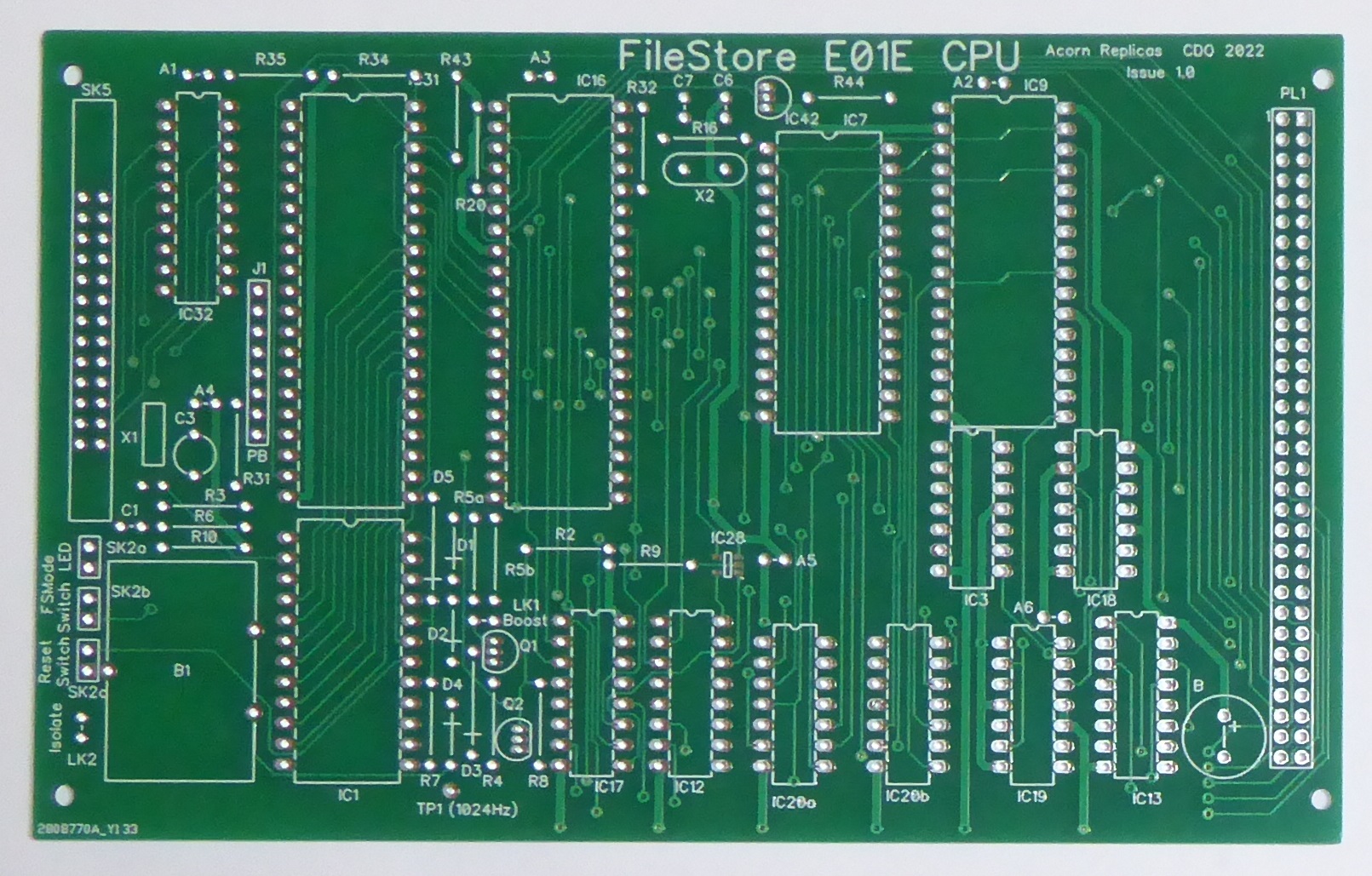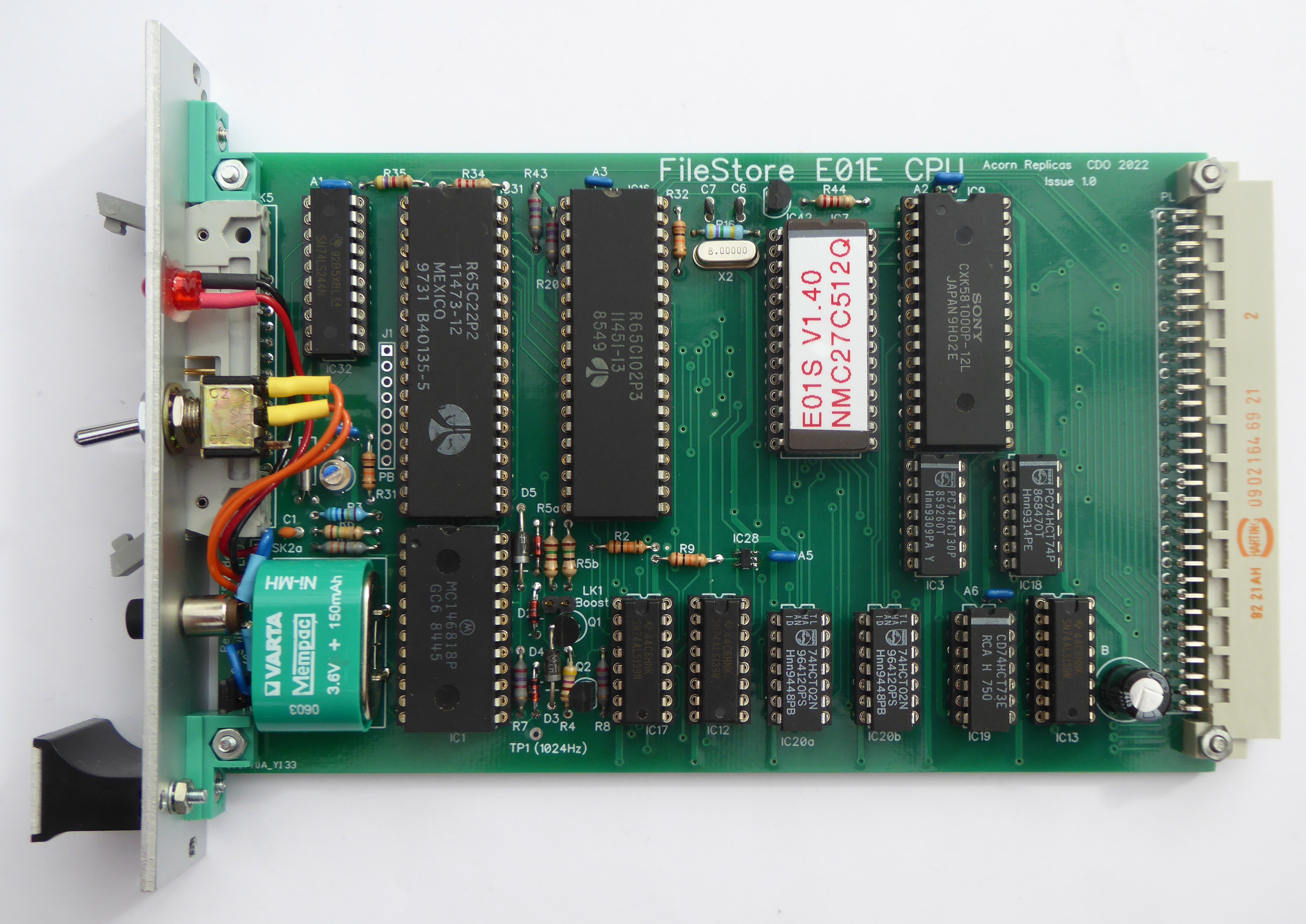
This board includes the CPU, RAM, EPROM, RTC and Printer Port together with all the address decoding.
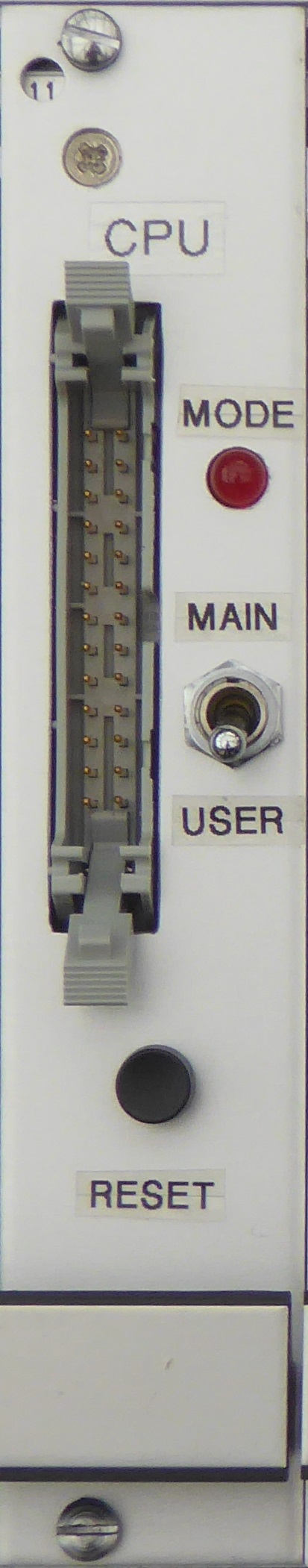
The CPU is a 65C102 running at 2MHz, I have added a Microchip MCP120 Microcontroller Supervisory Chip to generate system reset, there is provision for a front panel mounted reset switch via SK2c.
The EPROM is as the E01S, a single 27512 64K x 8-bits. I have removed the DRAM memory and replaced it with a single 128k x 8-bit SRAM although only half is used, this simplified the circuit considerably and also makes it possible to fit it all on a standard sized (100x160mm) Eurocard.
Either the 'A' version or non 'A' version of the MC146818 RTC can be used (Issue 1.0 boards will require a link to tie pin 1 to 0V to use the 'A' version). The RTC requires battery backup, the E01S used a plug-in 3.6V NiCd module, I have replaced this with a PCB mounted NiMH pack. I have adjusted component values in the charging circuit to account for the different chemistry and added a 'boost' link, LK1, which enables a completely flat battery to be charged more quickly (this link should not be left fitted for longer than 8 hours to avoid damage to the battery).
The original NiCd circuit trickle charged at a nominal 15mA, the Varta 3.6V NiMH cell with a capacity of 150mAhr (CA) should be trickle charged at 0.03CA (4.5mA) and can be charged at a higher rate of 0.2CA (30mA) for up to 8 hours.
Access to the RTC is enabled by bit 3 of the FDC Latch (Acorn call it the 'Miscellaneous Function Latch'), as this is on the FDC Board I have had to replicate this bit of the latch using a spare 74HCT73 latch (IC6.1).
A spare Econet line driver (26LS30 IC28) was originally used to 'read' the door switch I have replaced this with a single gate 74VHC1GT125 (IC 28), the front panel mounted 'door switch' or FSMode switch is then connected to SK2b.
The E01S front panel (red) FS Mode LED is driven again by a bit of the FDC Latch on the FDC Board, I have routed this signal via the backplane to this board as it seemed more logical for it to be on the CPU front panel (via SK2a).
Address decoding is as the original E01S although gate reference numbers have had to be swapped a bit to enable PCB tracking etc.
Both the EPROM (IC7) and RAM (IC9) occupy the entire 64K memory space, although the page $FC00 will always access memory mapped I/O. After reset a read will access the EPROM, a write will access the RAM. Writing to the ROM latch (IC6) will switch out the EPROM so from then on all reads also come from the RAM (the EPROM cannot be switched back in other than via a reset).
Memory Mapped I/O
| Address Range | Function |
| $FC00 (- $FC03) | RTC Address Register |
| $FC04 (- $FC07) | RTC Data Register |
| $FC08 (- $FC0B) | FDC Latch (aka Miscellaneous Functions
Latch) reading this location will switch out the EPROM writing updates the latch |
| $FC0C - FC0F | Floppy Disk Controller (FDC) |
| $FC10 - $FC1F | 6522 VIA (Printer Port) |
| $FC20 - $FC23 | 6854 Econet Interface |
| $FC24 (- $FC27) | Econet Interrupt Disable |
| $FC28 (- $FC2B) | Econet Interrupt Enable |
| $FC2C (- $FC2F) | Floppy Drive Door Switch state (FSMode) |
| $FC30 - $FC33 | SCSI Interface |
| Register Address | Register Name | Function |
| $FC11 | IORA | Input / Output Register A |
| $FC13 | DDRA | Data Direction Register A |
| $FC14 | T1CL | Timer 1 Counter Low |
| $FC15 | T1CH | Timer 1 Counter High |
| $FC1B | AUXCR | Auxiliary Control Register |
| $FC1C | PCR | Peripheral Control Register |
| $FC1D | IFR | Interrupt Flag Register |
| $FC1E | IER | Interrupt Enable Register |
RTC MC156818 (IC1) Registers
Registers $00 to $0D access the Real Time Clock, Registers $0E to $3F are non-volatile memory (battery backed-up)
| Register Address | Function |
| $00 | seconds 0-59 |
| $01 | seconds alarm 0-59 |
| $02 | minutes 0-59 |
| $03 | minutes alarm 0-59 |
| $04 | hours 1-2 or 0-23 |
| $05 | hours alarm 1-2 or 0-23 |
| $06 | day of the week 1-7 (1=Sunday) |
| $07 | date 1-31 |
| $08 | month |
| $09 | year |
| $0A | bit 0-3: Rate Selection
bits (RS0-3), 0110=1024Hz bits 4-6: clock DiVider bits (DV0-2), 010=32.768kHz bit 7: Update In Progress (UIP), 1=busy |
| $0B | bit 0: Daylight Saving
Enable (DSE), 0=disabled bit 1: 24/12, 1=24 bit 2: Data Mode (DM), 1=binary bit 3: Square Wave output Enable (SQWE), 1=enabled bit 4: Update-ended Interrupt Enable (UIE), 1=enabled bit 5: Alarm Interrupt Enable (AIE), 0=disabled bit 6: Periodic Interrupt Enable (PIE),0=disabled bit 7: SET, 0=disabled |
| $0C | bits 0-3: unused bit 4: UF Update-ended Interrupt Flag bit 5: AF Alarm Interrupt Flag bit 6: PF Periodic Interrupt Flag bit 7: IRQF Interrupt Request Flag |
| $0D | bits 0-6: unused bit 7: VRT Valid RAM and Time bit |
| $0E | Server Station number |
| $0F | 2's complement of Server Station number (used as a check) |
| $10-$13 | Reserved for use by MOS |
| $20 | on error - error code |
| $21 | on error - X |
| $22 | on error - Y |
| $23,$24 | on error address (MSB,LSB) |
| $19-$1B | on error - 24-bit SIN |
| $1C | maximum number of concurrent users (MAXUSERS) |
| $1D | the number of configured drives + 1 (MAXDRIVE) |
| $1E-$23 | printer server name (up to 6 characters), if $30=0 disable |
| $24-$2E | Maintenance Mode username |
| $2F | check byte for maintenance username |
| $30 | printer page feed, 0=o |
| $31 | disables hard disk copyright check if not 0 |
| $32-$3F | unused |
Schematic
Bill Of Materials
Front Panel
PCB